
Back to Faculty Directory
jamie.warner@austin.utexas.edu
Office Location: EER 6.620
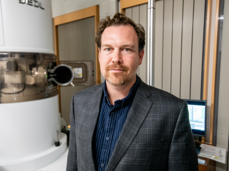
Jamie Warner
Professor
Temple Foundation Endowed Professorship No. 1
Department Research Areas
Advanced Materials Science and Engineering
TMI Electron Microscopy Facility
Dr. Jamie H. Warner joined the Walker Department of Mechanical Engineering at The University of Texas at Austin in January 2020 to lead the new Electron Microscopy Facility located in the Engineering Education and Research Center, Texas Materials Institute and the Cockrell School of Engineering. Prior to this he spent 13 years in the Department of Materials at the University of Oxford, where he held the position of Professor of Materials and led the Nanostructured Materials Group. His research focuses on the next generation of nanostructured materials with unique properties that will impact electronic, opto-electronic, and energy applications. The core foundation of his research is on the atomic level structure and dynamics of nanomaterials realized through state-of-the-art aberration-corrected transmission electron microscopy and spectroscopy. A wide range of nanoscale characterization tools (TEM, SEM, AFM, FIB) are also used to probe materials across all dimension scales. New types of nanoscale opto-electronic devices are produced in clean-room nanofabrication facilities, utilizing materials ranging from 2D Crystals (graphene, BN, MoS2, WS2 etc), 1D wires and nanotubes, to 0D quantum dots.
He completed a PhD in Physics at the University of Queensland in 2004, and then spent 18 months as a post-doc in New Zealand and Australia, before moving to the Department of Materials at Oxford in November 2006. In October 2008, He was awarded the University of Oxford's Glasstone Fellowship in Science to start an independent research group. At this same time, he began a Kurti Junior Research Fellowship in Science at Brasenose College. In October 2010, he was awarded a Royal Society University Research Fellowship in the topic of nanomaterials and electron microscopy. From October 2011-2014, he was also a Governing body member of Balliol College, as a Research Fellow in Science. In September 2012, he moved from Senior Research Fellow to Academic Staff, a 'Research Lecturer' in the Department of Materials. In May 2014, he became Associate Professor in the Department of Materials at the University of Oxford. In July 2014, he was promoted to Full Professor in the Department of Materials in Oxford.
In Fall 2014, he was a Visiting Professor at MIT in the Department of Chemical Engineering, and during 2016 he spent the Fall term as Visiting Professor in the Department of Materials Sciences and Engineering at MIT, teaching a special options postgraduate course on 2D Materials and undertaking extensive research collaborations with faculty. He was a visiting Professor at Sungkyunkwan University in Korea from 2014-2018, teaching a post-graduate course on 2D materials for Energy and Opto-Electronic Applications. He is currently a Visiting Professor at the University of Oxford. He graduated 30 PhD students during his time at the University of Oxford.
In 2019, he became a Fellow of the Royal Society of Chemistry. In 2017, he was awarded an ERC Consolidator Grant for 5 years on Large Area Transparent Opto-Electronics. In 2018, he was listed as one of the top 10 ‘highly prolific’ authors for ACS Nano since its inception. In 2019 he was the ACS Nano Lectureship winner. He is the Editor-in-Chief of the journal Materials Today Advances, and is on the Editorial Boards of Materials Today, Materials Today Chemistry, Applied Materials Today, Materials Today Nano, and Materials Today Energy. In 2020 he joined the Editorial Advisory Board of ACS Nano.
He has >300 peer reviewed publications, with >160 as the corresponding author, including Science, Nature Materials, Nature Nanotechnology, Nature Communications (x3), Nano Letters (x16), Advanced Materials (x4), ACS Nano (x60), on the topics of nanomaterials for opto-electronics, energy, bio-applications, and quantum materials. Jamie Warner’s google scholar citations.
Recent Publications
- S. Sinha, T. Zhu, A. France-Lanord, Y. Sheng, J. C. Grossman, K. Porfyrakis, J. H. Warner, Atomic Structure and Defect Dynamics of Monolayer Lead Iodide Nanodisks with Epitaxial Alignment on Graphene, Nature Communications, Accepted in press (2020).
- Y. Lu, J. Chen, T. Chen, Y. Shu, R-J. Chang, Y. Sheng, V. Shautsova, N. Mkhize, P. Holdway, H. Bhaskaran, J. H. Warner, Controlling Defects in Continuous 2D GaS Films for High Performance Wavelength-Tunable UV-Discriminating Photodetectors, Advanced Materials, Early View, doi.org/10.1002/adma.201906958 (2020).
- J. Chen, G. H. Ryu, Q. Zhang, Y. Wen, K-L. Tai, J. H. Warner, Spatially Controlled Fabrication and Mechanisms of Atomically Thin Nanowell Patterns in Bilayer WS2 using In-situ High Temperature Electron Microscopy, ACS Nano, 13, 14486-14499, (2019).
- J. Chen, G. Ryu, S. Sapna, J. H. Warner, Atomic Structure and Dynamics of Defects and Grain Boundaries in 2D Pd2Se3 Monolayers, ACS Nano, 13, 8256-8264, (2019).
- G. H. Ryu, T. Zhu, J. Chen, S. Sinha, V. Shautsova, J. C. Grossman, J. H. Warner, Striated 2D Lattice with Sub-nm Etch Channels by Controlled Thermally Induced Phase Transformations of PdSe2, Advanced Materials, 31, 1904251, (2019).
- Y. Wen, C. Ophus, C. S. Allen, S. Fang, J. Chen, E. Kaxiras, A. I. Kirkland, J. H. Warner, Simultaneous Identification of Low and High Atomic Numbers in Monolayer 2D Materials using 4D Scanning Transmission Electron Microscopy, Nano Letters, 19, 6482-6491, (2019).
- S. Fang, Y. Wen, C. S. Allen, C. Ophus, G. G. D. Han, A. I. Kirkland, E. Kaxiras, J. H. Warner, Atomic Electrostatic Maps of 1D Channels in 2D Semiconductors using 4D Scanning Transmission Electron Microscopy, Nature Communications 10, 1127, (2019).
- A. G. Rajan, K. S. Silmore, J. Swett, A. W. Robertson, J. H. Warner, D. Blankschtein, M. S. Strano, Addressing the Isomer Cataloging Problem for Nanopores in Two-Dimensional Materials. Nature Materials, 18, 129-135, (2019).
- G. S. Jung, S. Wang, Z. Qin, S. Zhou, M. Danaie, A. I. Kirkland, M. J. Buehler, J. H. Warner, Anisotropic Fracture Dynamics Due to Local Lattice Distortions, ACS Nano, 13, 5693-5702, (2019).
- Y. Sheng, T. Chen, Y. Lu, R-J. Chang, S. Sinha, J. H. Warner, High-Performance WS2 Monolayer Light-Emitting Tunneling Devices Using 2D Materials Grown by Chemical Vapour Deposition, ACS Nano, 13, 4530-4537, (2019).
- Q. Chen, H. Li, S. Zhou, W. Xu, J. Chen, H. Sawada, C. S. Allen, A. I. Kirkland, J. C. Grossman, J. H. Warner, Ultralong 1D Vacancy Channels for Rapid Atomic Migration during 2D Void Formation in Monolayer MoS2, ACS Nano, 12, 7721-7730 (2018).
- H. Tan, W. Xu, Y. Sheng, Y. Fan, Q. Chen, M. Tweedie, X. Wang, Y. Zhou, J. H. Warner, Lateral Graphene Contacted Vertically Stacked WS2/MoS2 Hybrid Photodetectors with Large Gain, Advanced Materials, 29, 1702917, (2017).
- G. Liu, A. W. Robertson, M. M-J Li, W. C. H. Kuo, M. T. Darby, M. H. Muhieddine, Y-C Lin, K. Suenaga, M. Stamatakis, J. H. Warner, S. C. E. Tsang, MoS2 monolayer catalyst doped with isolated Co atoms for the hydro-deoxygenation reaction, Nature Chemistry, 9, 810-816, (2017).
